
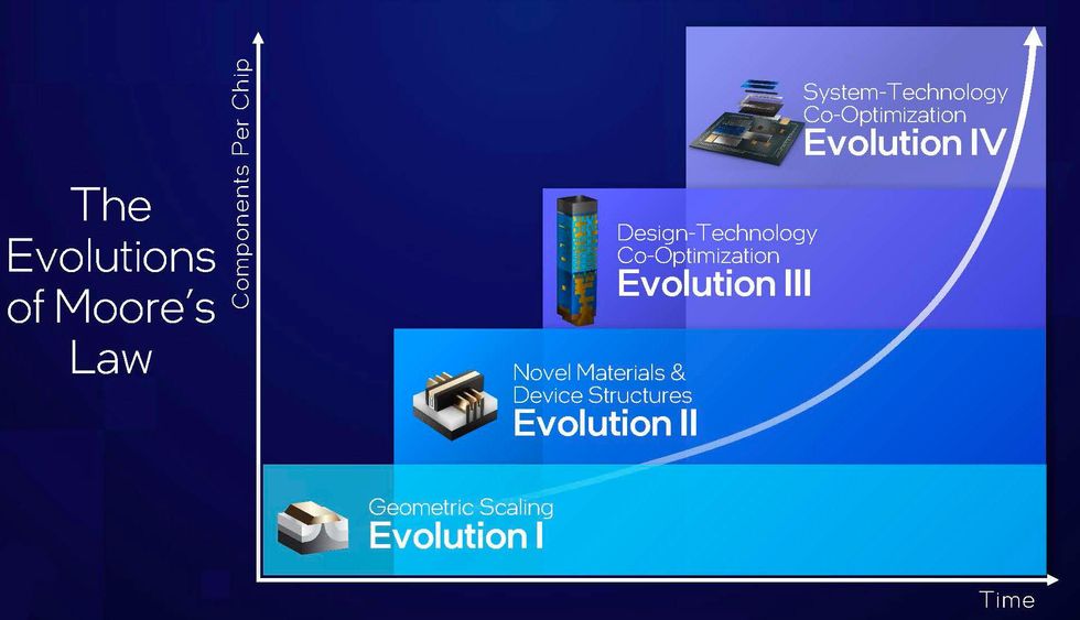
The up coming wave of Moore’s Law will rely on a acquiring principle termed technique know-how co-optimization, stated Ann B. Kelleher, basic supervisor of technology growth at Intel in an job interview with IEEE Spectrum forward of her plenary chat at the 2022 IEEE Electron Device Assembly (IEDM).
“Moore’s Regulation is about escalating the integration of functions,” claims Kelleher. “As we glance ahead into the following 10 to 20 years, there’s a pipeline full of innovation” that will continue on the cadence of enhanced goods each two a long time. That path contains the normal ongoing advancements in semiconductor procedures and layout, but method technologies co-optimization (STCO) will make the most important change.
Kelleher calls it an “outside-in” way of advancement. It starts with the workload a product or service requires to support and its program, then performs down to procedure architecture, then what variety of silicon ought to be within a offer, and last but not least down to the semiconductor production system. “With method technological innovation co-optimization, it suggests all the pieces are optimized jointly so that you’re finding your best respond to for the finish product or service,” she suggests.
 Ann B. KelleherIntel
STCO is an option now in massive portion simply because sophisticated packaging, these as 3D integration, is allowing for the superior-bandwidth relationship of chiplets—small, practical chips—inside a solitary package. This suggests that what would after be capabilities on a one chip can be disaggregated on to dedicated chiplets, which can just about every then be made making use of the most exceptional semiconductor process know-how. For case in point, Kelleher details out in her plenary that substantial-effectiveness computing needs a huge amount of cache memory per processor core, but chipmaker’s potential to shrink SRAM is not continuing at the exact speed as the scaling down of logic. So it will make sense to develop SRAM caches and compute cores as separate chiplets working with unique procedure technology and then stitch them with each other making use of 3D integration.
A crucial case in point of STCO in motion, claims Kelleher, is the Ponte Vecchio processor at the heart of the Aurora supercomputer. It is composed of 47 energetic chiplets (as well as 8 blanks for thermal conduction). These are stitched together applying both innovative horizontal connections (2.5D packaging tech) and 3D stacking. “It delivers with each other silicon from diverse fabs and allows them to arrive collectively so that the process is equipped to conduct versus the workload that it’s intended for,” she claims.
 Intel sees a idea known as process know-how co-optimizaiton as the up coming phase of Moore’s Regulation.Intel
At IEDM, Intel engineers will report that they’ve enhanced the density of their 3D hybrid bonding technologies tenfold vs . what they documented in 2021. Amplified link density usually means far more chip functions can be disaggregated onto different chiplets, in switch furnishing a lot more prospective to use STCO to strengthen outcomes. Hybrid bond pitches, meaning the length among the interconnects, are just 3 micrometers with this new know-how. With that, even much more cache can be separated from the processor cores. Decreasing the bond pitch to involving 2 micrometers and 100 nanometers could necessarily mean staying capable to begin pulling aside logic functions that today must be on the same piece of silicon, in accordance to Kelleher.
The travel to improve units by disaggregating capabilities is acquiring effects for potential semiconductor manufacturing processes. Future semiconductor method know-how has to contend with the thermal stresses of a 3D-packaged surroundings. But interconnect technological innovation will likely see the largest transform. Kelleher suggests Intel is on observe to introduce a technological innovation it calls PowerVia (backside electric power shipping and delivery, additional generally) in 2024. PowerVia moves a chip’s energy delivery community beneath the silicon, reducing the sizing of logic cells and reducing electric power consumption. But it also “gives us unique options in phrases of what we can and how we can interconnect in the package,” states Kelleher.
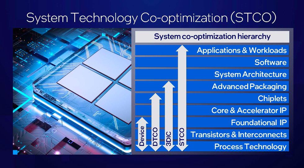 Program engineering co-optimization (STCO) optimizes additional of a laptop procedure by using all the things into account from software program to procedure technological innovation.Intel
Kelleher stresses that STCO is however in its infancy. Electronic design and style automation (EDA) applications have already tackled STCO’s predecessor, design technology co-optimization (DTCO), which focuses on logic-mobile amount and functional-block amount optimizations. “But some of the EDA software sellers are now performing on this,” she states. “Going ahead, the emphasis is going to be on the methods and tools that help help STCO.”
As STCO develops, unit engineers may well have to establish with it. “Generally, engineers will will need to keep on to have their system understanding but also get started to understand the use scenarios of their engineering and their units,” claims Kelleher. “More interdisciplinary techniques will be needed as we head into much more of an STCO earth.”
Intel’s Road Map
Kelleher also updated Intel’s street map, tying it in with the progression of Moore’s Legislation and the evolution of the device given that the creation of the first transistor. The base line is that items are on keep track of from when Intel introduced its new production street map fewer than two decades ago, according to Kelleher. But she did fill in some specifics of which processors would debut with the new tech.
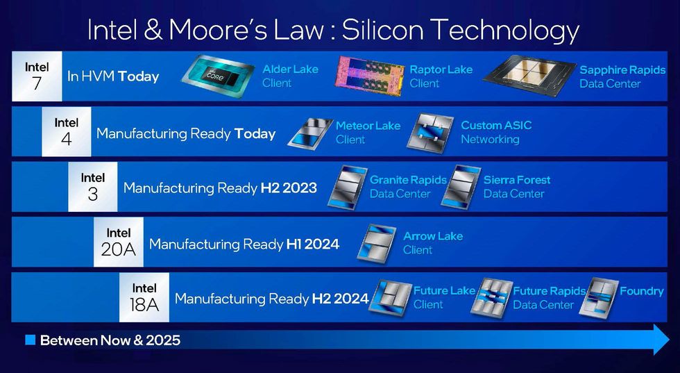 Intel is on schedule with its process technological innovation highway map.Intel
Intel 20A, owing for manufacturing introduction in the initially 50 percent of 2024, continues to be the significant technological jump. It concurrently introduces a new transistor architecture—RibbonFET (much more normally identified as gate-all-close to or nanosheet transistors)—and PowerVia backside ability shipping and delivery. Requested about the possibility concerned, Kelleher described the approach.
“They do not have to be performed at when, but we see important benefits from transferring to PowerVia to permit the [RibbonFET] technological know-how,” she suggests. The advancement is happening in parallel to decrease the risk of delays, she clarifies. Intel is working a examination approach making use of FinFETs, the transistor architecture in use currently, with PowerVia. “That has been performing incredibly properly and it has enabled us to accelerate our enhancement perform,” she suggests.
The Transistor of the Potential
Kelleher’s converse arrives as the IEEE Electron Device Society celebrates the 75th anniversary of the invention of the transistor. At IEEE Spectrum, we asked gurus what the transistor might be like on its 100th birthday in 2047. Kelleher’s just take took in the extensive lifetimes of transistor technological innovation, noting that the planar transistor layout lasted from 1960 to about 2010, and that its successor the FinFET is nonetheless likely strong. “Now we’re going to the RibbonFET which is likely to last for possibly another 20-moreover years…so I hope we’re going to be somewhere with stacked RibbonFETs,” she proposed. [Intel engineers describe that technology in the December 2022 issue of IEEE Spectrum.] Even so, by that time, the ribbons could be made of 2D semiconductors in its place of silicon.
From Your Web page Article content
Relevant Articles About the Internet


